This series is based on the Nand2Tetris course. Quoted materials are © their original authors. This project is not affiliated with or endorsed by Nand2Tetris.
In this series, we’ll build a modern computer from the ground up, starting with a single NAND gate. This article introduces the boolean logic needed to build the digital circuits used in all computers. You can find all the course materials on the official Nand2Tetris website.
Table of contents
Open Table of contents
A bit of theory
If you wish to skip this section, directly jump to Building the gates
What is boolean logic
Before getting started with implementing boolean logic in hardware, we have to understand what it is exactly. Boolean logic (or boolean algebra) is a branch of algebra where there are only two possible values: true and false, usually denoted by 1 and 0, whereas elementary algebra uses numbers. Furthermore, boolean algebra uses logical operators while elementary algebra uses arithmetic operators.
Each binary variable has 2 possible states. with N variables, we get 2^n combinations.
Elementary operations
In order to represent boolean operations, we use the following symbols:
&for AND|for OR~for NOT
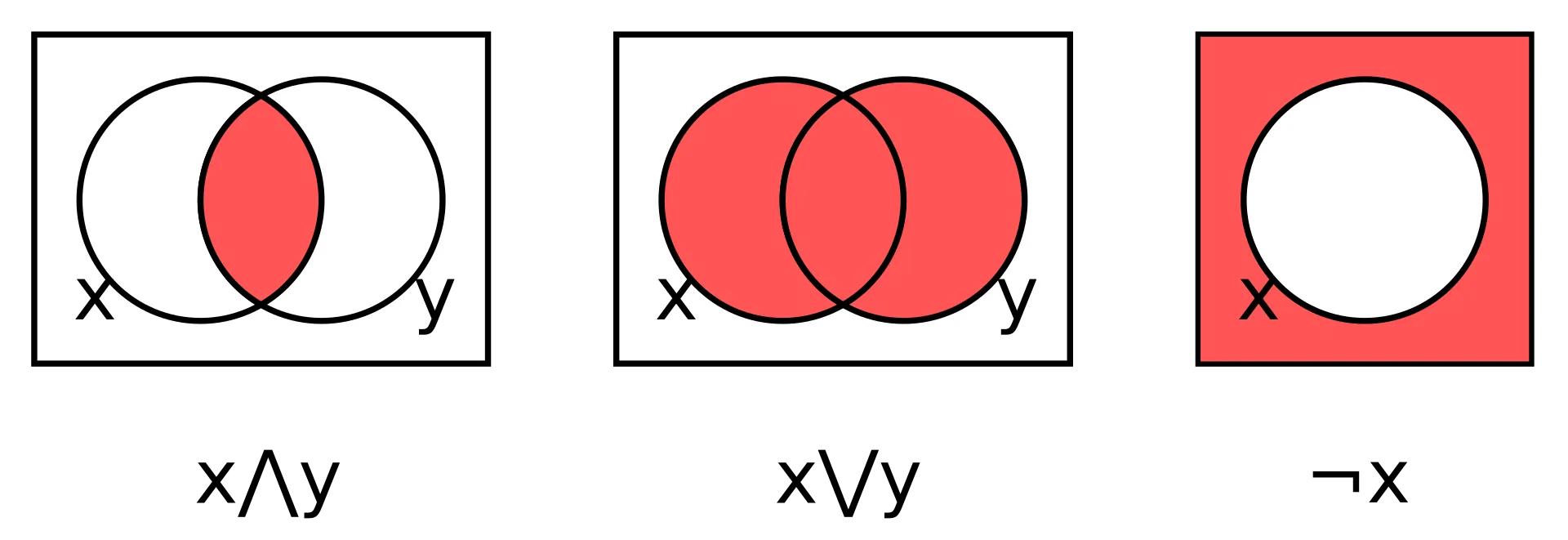 Figure 1: A diagram representing the three elementary operations.1
Important laws of boolean logic
In boolean algebra, the associative and commutative laws are true. However, there are three more important laws that aren’t used in elementary algebra:
-
~(A & B) = ~A | ~B
~(A | B) = ~A & ~B
If you’re familiar with set theory, De Morgan’s laws are just a formality for you. If it’s not the case, you can find more information in my introduction to set theory.
-
A & (B | A) = A A | (B & A) = A -
A & (B | C) = (A & B) | (A & C)
A | (B & C) = (A | B) & (A | C)
Please refer to my boolean algebra cheat sheet for more information about all the laws of boolean algebra and their proofs.
Representing boolean functions
To understand how boolean logic works, we can represent it with truth tables. A truth table is a table that shows the truth value of each possible combination of inputs. For example, the truth table for the AND operation is shown in Figure 2.
| x | y | Output |
|---|---|---|
| 0 | 0 | 0 |
| 0 | 1 | 0 |
| 1 | 0 | 0 |
| 1 | 1 | 1 |
Figure 2: Truth table for the AND operation.
We observe that the output of the AND operation is 1 when both inputs are 1, and 0 otherwise.
We consider the following truth table for the OR operation:
| x | y | Output |
|---|---|---|
| 0 | 0 | 0 |
| 0 | 1 | 1 |
| 1 | 0 | 1 |
| 1 | 1 | 1 |
Figure 3: Truth table for the OR operation.
Notice that the output of the OR operation is 1 when either input is 1, and 0 otherwise. There is no need to look at the truth table for the NOT operation since its output is simply the opposite of the input.
With that in mind, we now represent more complex boolean functions.
Let’s try to write the truth table for the following function:
f(x, y) = (x & ~y) | (~x & y)To make things easier, we’ll split the main function into two smaller functions: f1(x, y) = x & ~y and f2(x, y) = ~x & y. The truth table for both functions is shown in Figures 4 and 5.
| x | y | Output |
|---|---|---|
| 0 | 0 | 0 |
| 0 | 1 | 0 |
| 1 | 0 | 1 |
| 1 | 1 | 0 |
Figure 4: Truth table for the function f1(x, y) = x & ~y.
| x | y | Output |
|---|---|---|
| 0 | 0 | 0 |
| 0 | 1 | 1 |
| 1 | 0 | 0 |
| 1 | 1 | 0 |
Figure 5: Truth table for the function f2(x, y) = ~x & y.
Combining the outputs of f1 and f2 with the OR operator gives us the final function. Its truth table is as follows:
| x | y | Output |
|---|---|---|
| 0 | 0 | 0 |
| 0 | 1 | 1 |
| 1 | 0 | 1 |
| 1 | 1 | 0 |
Figure 6: Truth table for the function.
We observe that the output of the function is 1 when only one of the inputs is 1, and 0 otherwise. This function is called the XOR operation (exclusive OR written as ^ or ⊕).
Now that we know how to build functions using logic operations, we are ready to see how they can be simplified to optimize hardware implementation.
Simplifying boolean functions
Now we simplify the following function using two different methods: algebraic simplification and Karnaugh map.
f(x, y, z) = x & y | x & ~y & z | ~x & y & zWe’ll first use algebraic methods, based on the laws previously introduced.
Algebraic simplification
Apply distribution to the first two terms:
x & (~y & z | y) | ~x & y & zUse absorption:
x & (y | z) | ~x & y & zDistribute again:
x & y | x & z | ~x & y & zFactoring:
x & y | z (~y & x | y)Reduce again using absorption:
x & y | z (x | y)Final expression:
x & y | z & x | z & yThe simplified function produces identical outputs to the original, despite its reduced complexity.
Don’t hesitate to find the truth table of this new function and compare it with the original one.
Another powerful tool for simplification — especially when dealing with a lot of variables — is the Karnaugh map.
Karnaugh map
Consider the following truth table:
| x | y | z | f(x, y, z) |
|---|---|---|---|
| 0 | 0 | 0 | 0 |
| 0 | 0 | 1 | 0 |
| 0 | 1 | 0 | 0 |
| 0 | 1 | 1 | 1 |
| 1 | 0 | 0 | 0 |
| 1 | 0 | 1 | 1 |
| 1 | 1 | 0 | 1 |
| 1 | 1 | 1 | 1 |
Figure 7: Truth table for the function.
The Karnaugh map uses Gray code ordering to ensure that only one variable changes between adjacent cells. In a 3-variable K-map, we usually place x on one axis and combine y and z on the other.
To fill the Karnaugh map, we need to follow the truth table and fill the corresponding cells. For example, the cell (0, 0, 0) is filled with the output 0, and the cell (1, 1, 1) is filled with the output 1. In the event where no output is expected, we can mark the cell with a * (don’t care cell).
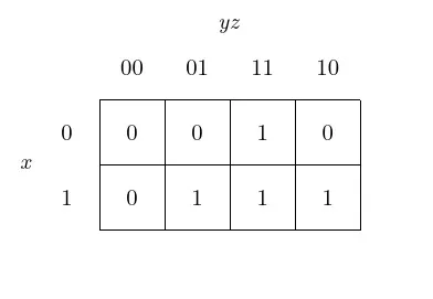
Figure 8: The Karnaugh map for the function.
Once the map is filled, we find all the 1s and group them. A group is a set of adjacent 1s (including possible “don’t care” cells) forming a rectangle of 1, 2, 4, or 8 cells. Overlapping is allowed, and larger groups lead to simpler expressions. In our case, we find 3 groups: (5, 7), (3, 7) and (6, 7).2
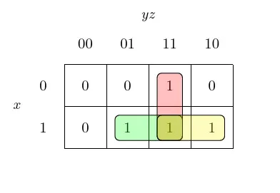
Figure 9: The Karnaugh map with the groups.
After obtaining the groups, we find their equations and thus find the simplified function as follows:
- Green:
x & z - Red:
y & z - Yellow:
x & y
To obtain the simplified function, we join the equations using the OR operator.
f(x, y, z) = x & z | y & z | x & yThis concludes the Karnaugh map method. We have simplified the function using two different methods: algebraic simplification and Karnaugh map. Notice that both methods give the same result but the thought process is different. I prefer the Karnaugh map because it is much easier to understand and allows to work on larger functions.
Ultimately, we managed to reduce the amount of logic gates needed to implement the function from 9 to 5.
Find more about Karnaugh maps on this MIT OCW page.
Conclusion on boolean logic
Boolean algebra is the foundation of all digital systems. Understanding how to build and simplify logic functions is the first step toward designing CPUs, memory chips, and full computer architectures. In the second part of this post, we are moving from theory to practice by implementing these gates in HDL and testing them in hardware.
Building the gates
All the HDL files with detailed explanations for this post can be found on my GitHub repository.
For this first project, we are tasked with building a variety of gates:
All the gates must be built starting from one single gate: the NAND gate. We can do so because any boolean function can be expressed as a truth table, and any truth table can be expressed as a boolean function using only NOT, AND, and OR. This is called Disjunctive Normal Form (DNF).
The NAND gate
The NAND gate is the inverse of the AND gate. It outputs 0 when both inputs are 1, and 1 otherwise.
| x | y | Output |
|---|---|---|
| 0 | 0 | 1 |
| 0 | 1 | 1 |
| 1 | 0 | 1 |
| 1 | 1 | 0 |
Figure 10: Truth table for the NAND gate.
Elementary gates
We begin by building the following gates:
NOT gate
The NOT gate inverts its input: 0 becomes 1, and vice versa. Since it only possesses one input, we will feed twice the same input into the NAND gate. If you have a look at the truth table for the NAND gate, you will see that the output is 0 when both inputs are 1, and 1 otherwise. This is exactly what we need! Hence, we use the NAND gate to implement the NOT gate as follows:
NOT(x) = NAND(x, x)AND gate
We already saw that the AND gate returns 1 only when both inputs are 1. Using the NOT gate we just built, we can now express it with NAND:
AND(x, y) = NOT(NAND(x, y)) = NAND(NAND(x, y), NAND(x, y))OR gate
The OR gate outputs 1 when at least one of the inputs is 1, and 0 otherwise.
Initially, I struggled to see how an OR gate could be built using only NAND-based NOT and AND gates. Then I recalled De Morgan’s laws, which provide a way to express OR using only AND and NOT.
Apply De Morgan’s law
x | y = ~~x | ~~y = ~(~x & ~y)This leads to the following expression for the OR gate:
OR(x, y) = NOT(AND(NOT(x), NOT(y))) = NAND(NAND(x, x), NAND(y, y))XOR gate
Even though the course already provides the formular, I worked it out myself as a reasoning exercise. The XOR gate outputs 1 when exactly one of the two inputs is 1. The output is true when either:
x = 1andy = 0x = 0andy = 1
We represent these two cases with the following subfunctions:
| x | y | f1(x, y) | f2(x, y) | Output |
|---|---|---|---|---|
| 0 | 0 | 0 | 0 | 0 |
| 0 | 1 | 0 | 1 | 1 |
| 1 | 0 | 1 | 0 | 1 |
| 1 | 1 | 0 | 0 | 0 |
Figure 11: Truth table for the functions f1(x, y), f2(x, y) and the XOR gate
Following the truth table, we write the formulas for f1 and f2:
f1(x, y) = ~x & y
f2(x, y) = x & ~y
We then combine the output of both functions f1 and f2 using the OR operation, resulting in the XOR gate:
XOR(x, y) = OR(AND(NOT(x), y), AND(x, NOT(y)))Composite gates
We now use the elementary gates to build more complex components:
Multiplexer
     +-----------+
a ---|1          |
     |      MUX  |--- Out	 		/* Simple schema of a 2 to 1 multiplexer */
	 |           |
b ---|0          |
     +-----------+
            |
            S
A multiplexer (MUX) is a fundamental building block in digital circuits: it selects one of several input signals and forwards it to the output. In our case, we’re building a 2-to-1 MUX, which routes either input a or b to the output depending on the selector bit sel.
We write the truth table for the multiplexer:
| sel | a | b | Out |
|---|---|---|---|
| 0 | 0 | 0 | 0 |
| 0 | 0 | 1 | 0 |
| 0 | 1 | 0 | 1 |
| 0 | 1 | 1 | 1 |
| 1 | 0 | 0 | 0 |
| 1 | 0 | 1 | 1 |
| 1 | 1 | 0 | 0 |
| 1 | 1 | 1 | 1 |
Figure 12: Truth table for the 2 to 1 multiplexer
To find the corresponding boolean expression, we use a Karnaugh map based on the truth table above.
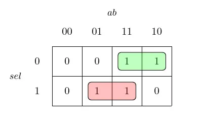
Figure 13: Karnaugh map with the groups for the 2 to 1 multiplexer
We then get the following boolean expressions:
- Green:
~sel & a - Red:
sel & b
These two expressions cover the cases when sel = 0 and sel = 1. We combine them using the OR operator to get the full function.
f(sel, a, b) = ~sel & a | sel & bThis gives the final formula for the 2 to 1 multiplexer:
MUX(a, b, sel) = OR(AND(NOT(sel), a), AND(sel, b))Now that we’ve implemented a data selector, we explore its inverse: the demultiplexer, which distributes a single input to multiple outputs.
Demultiplexer
      +-------+
in ---|       |--- a
      | DMUX  |					/* Simple schema of a 2 to 1 demultiplexer */
      |       |--- b
      +---┬---+
          |
         Sel
The demultiplexer (DMUX) is as important as the multiplexer: it sends the input to a specific output depending on the selector bit. In our case, we’re building a 2-to-1 DMUX, which routes the input to a specific output a or b depending on the selector bit sel.
The truth table for the demultiplexer is as follows:
| sel | In | a | b |
|---|---|---|---|
| 0 | 0 | 0 | 0 |
| 0 | 1 | 1 | 0 |
| 1 | 0 | 0 | 0 |
| 1 | 1 | 0 | 1 |
Figure 14: Truth table for the 2 to 1 demultiplexer
We directly write the boolean expression for the two outputs:
a = ~sel & inb = sel & in
This gives us the final logic for the demultiplexer:
DMUX(in, sel):
	a = AND(NOT(sel), in)
	b = AND(sel, in)
Multi-input gates
In this last part, we will rebuild all the gates to be able to handle more inputs.
- 16 bit NOT gate
- 16 bit AND gate
- 16 bit OR gate
- 16 bit multiplexer
- 8 inputs OR gate
- 4 inputs 16 bit multiplexer
- 8 inputs 16 bit multiplexer
- 4 inputs demultiplexer
- 8 inputs demultiplexer
To extend these gates to 16 bits, we apply the same logic bit by bit. For each type of gate: NOT, AND, OR, we use 16 copies of the corresponding 1 bit gate.
16 bit NOT gate
NOT16(a[15]):				/* a is a 16-bit input */
	out[0] = NOT(a[0])
	...
	out[15] = NOT(a[15])
16 bit AND gate
AND16(a[15], b[15]):
	out[0] = AND(a[0], b[0])
	...
	out[15] = AND(a[15], b[15])
16 bit OR gate
OR16(a[15], b[15]):
	out[0] = OR(a[0], b[0])
	...
	out[15] = OR(a[15], b[15])
16 bit multiplexer
Here, we use the 2 to 1 multiplexer we built earlier. Only this time, the inputs will be 16 bit buses.
MUX16(a[15], b[15], sel):
	out[0] = MUX(a[0], b[0], sel)
	...
	out[15] = MUX(a[15], b[15], sel)
8 inputs OR gate
Now, we’re going to build an 8-inputs OR gate. To do so, we build a first layer of 4 OR gates to combine the 8 inputs into 4 intermediate outputs.
OR1 = OR(a[0], a[1])
OR2 = OR(a[2], a[3])
OR3 = OR(a[4], a[5])
OR4 = OR(a[6], a[7])
Next, two more OR gates combine the intermediate results, followed by a final OR to produce the output:
OR5 = OR(OR1, OR2)
OR6 = OR(OR3, OR4)

OR8WAY = OR(OR5, OR6)
4 inputs 16 bit multiplexer
For this exercise, we build a 4 input multiplexer that can handle 16 bit inputs. We already built a 16 bit 2 to 1 multiplexer that we will reuse. To do so, we will have to place two 16 bit 2 to 1 multiplexers, one for each input.
The tricky part here is to correctly redirect the inputs to the desired output. Luckily, we are given a very important hint:
out = a if sel = 00
      b if sel = 01
      c if sel = 10
      d if sel = 11
The first bit of the sel bus sel[0] can tell us whether the desired output is a or b or c or d.
Thus, we implement a first layer composed of two 16 bit 2 to 1 multiplexers:
MUXAB = MUX16(a, b, sel[0])
MUXCD = MUX16(c, d, sel[0])
Now that we are left with only 2 temporary outputs a or b and c or d, we need to determine which one to send to the output. This time, we’ll use the second bit of the sel bus sel[1]. When sel[1] = 0, we will get either a or c, and when sel[1] = 1, we will get either b or d. We just need one more 16 bit 2 to 1 multiplexer to get the final output.
4MUX16 = MUX16(MUXAB, MUXCD, sel[1])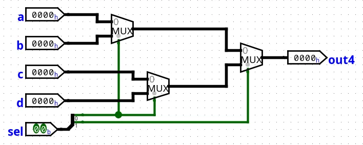
Figure 15: Diagram of a 4 inputs 16 bit multiplexer.
This gate requires combining several concepts introduced earlier as well as careful attention. There is another way to implement it, you can read about it on this Geeks for Geeks article.
8 inputs 16 bit multiplexer
Next, we build a 8-inputs 16 bit multiplexer by combining multiple 4 inputs 16 bit multiplexers. Just like before, we will split our inputs by using sel[0..1] as our first selector.
We can represent 4 different states on 2 bits. This allows us to drastically reduce the amount of inputs we send to the next layer.
Using two 16 bit 4 to 1 multiplexers:
MUXABCD = 4MUX16(a, b, c, d, sel[0..1])
MUXEFGH = 4MUX16(e, f, g, h, sel[0..1])
Now, we are left with 2 final buses: one belongs to a or b or c or d and the other belongs to e or f or g or h. We use a final 16 bit 2 to 1 multiplexer to get the desired output. Don’t forget to use sel[2] as our selector.
8MUX16 = MUX16(MUXABCD, MUXEFGH, sel[2])Here again, the tricky part was to determine which bits of
selto use as our selectors.
4 outputs demultiplexer
To finish this first project, we will work on multi-outputs demultiplexer. The first one we’ll build accepts a single bit input and sends it to one of its four outputs, depending on the two bits selector.
We begin by splitting our input into two temporary outputs: a or b or c or d. To do so, we use the first bit of our selector sel[1] with the 1 to 2 DMUX implemented earlier:
DMUX_SPLIT(in, sel):
	a = a or b
	b = c or d
Now that we have sorted in which bus the input belongs to (either a or b or c or d), we implement a second layer of 2 demultiplexers and our selector bit sel[0].
DMUXAB(in, sel):
	a = a or b[sel[0]]
	b = a or b[sel[0]]

DMUXCD(in, sel):
	a = c or d[sel[0]]
	b = c or d[sel[0]]
Finally, we obtain our complete 4 outputs demultiplexer:
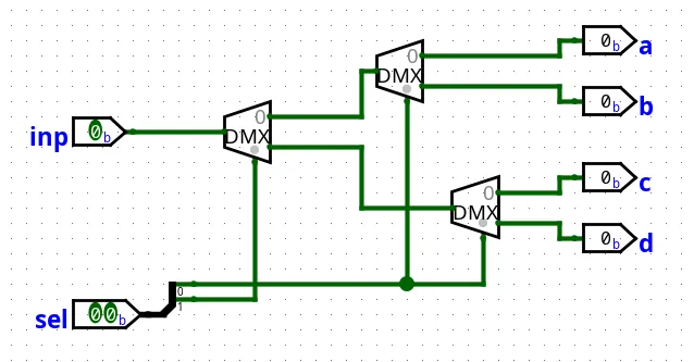
Figure 16: Diagram of a 4 outputs demultiplexer
8 outputs demultiplexer
The next step is to build the 8 outputs demultiplexer. As before, we’ll split our input into two temporary outputs: a or b or c or d and e or f or g or h using the first bit of our selector sel[2] with the 1 to 2 DMUX we implemented earlier.
DMUX_SPLIT(in, sel):
	a = a or b or c or d
	b = e or f or g or h
Now, we use two of our newly built 4 outputs demultiplexer to get our final 8 outputs demultiplexer. These demultiplexers will use the last two bits of our selector sel[0..1] as our selectors:
DMUXABCD(in, sel):
	a = a or b or c or d[sel[0..1]]
	b = a or b or c or d[sel[0..1]]

DMUXEFGH(in, sel):
	a = e or f or g or h[sel[0..1]]
	b = e or f or g or h[sel[0..1]]
And we have now successfully built our 8 outputs demultiplexer:
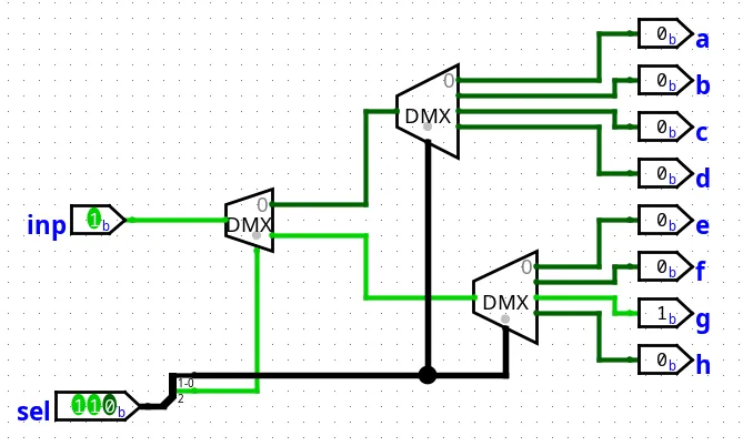
Figure 17: Diagram of a 8 outputs demultiplexer
Conclusion
This first project sets the ground for everything that follows. Logic gates aren’t just abstract concepts and theoretical definitions. They are real-world components that can be used to build complex circuits. Starting from boolean algebra, I build a small but complete set of logic components, starting from a single NAND gate.
More importantly, this project gave me a better understanding of how real hardware is designed: abstraction helps manage complexity, composition lets us build larger components from simple parts, and simplification directly reduces the number of gates, and thus the silicon area.
In the next article, we will move from logic gates to more advanced components, allowing us to build a fully functional ALU.
Footnotes
-
It is not rare to find the elementary expressions written with different symbols (∧ for AND, ∨ for OR, and ¬ for NOT). For more simplicity and readability, we use the more readable symbols presented at the beginning of this post. ↩
-
The values mentioned here are the base 10 numbers corresponding to the binary numbers formed by the 3 bits in the map. ↩